Tensor Core
GPU cores that operate on entire matrices with each instruction, providing the highest arithmetic throughput on NVIDIA GPUs since Volta.
Tensor Cores are GPU cores that operate on entire matrices with each instruction. Since their introduction in the Volta Streaming Multiprocessor (SM) Architecture, they have been the only way to reach the highest arithmetic throughput on NVIDIA GPUs, providing 100× more floating point operations per second than CUDA Cores.
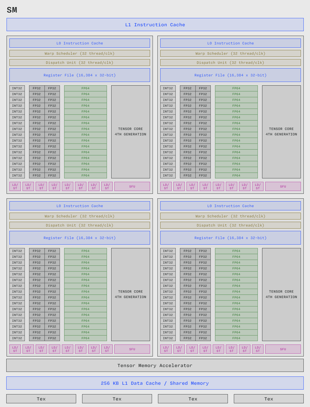
Key idea Operating on more data per instruction fetch dramatically reduces power requirements, which unlocks more performance (see this talk by Bill Dally, NVIDIA's Chief Scientist).
Reading a Tensor Core instruction#
Take the HMMA16.16816.F32 SASS instruction. It computes D = AB + C for matrices A, B, C and D, where C is often the same physical matrix as D.
MMAmeans "Matrix Multiply and Accumulate".HMMA16means the inputs are half precision (16 bit).F32means outputs are accumulated into 32 bit (single precision) floats.16816is not one number above 16,000. It is three dimensions:16,8and16.
NVIDIA usually names these dimensions m, n and k, for example in PTX instructions. The outer dimensions of A and B (m and n) come first, followed by the shared inner dimension for the accumulation (k). So this instruction performs 16 × 8 × 16 = 2,048 multiply-accumulate (MAC) operations.
A warp-wide, CISC-like instruction#
A single instruction in a single thread does not produce the whole matrix product. The 32 threads of a warp execute the instruction together and cooperatively produce the result.
Most of the per-instruction power overhead is in decoding, which the warp scheduler shares across the warp. Even spread across 32 threads, that's 2,048 ÷ 32 = 64 MACs per instruction.
So it helps to think of Tensor Cores, and similar hardware like the systolic arrays in Google's Tensor Processing Units (TPUs), as complex instruction set computer (CISC) hardware. For this perspective applied to TPUs, see this talk by computer architect David Patterson, who also coined the terms CISC and RISC.
From CUDA C++ to PTX to SASS#
SASS Tensor Core instructions are typically generated by the compiler from PTX matrix-multiply-and-accumulate instructions like wmma (documented here). These also compute D = AB + C, but are usually compiled into many SASS Tensor Core instructions that each operate on smaller matrices. CUDA C++ exposes the PTX instructions as intrinsics.
Here is the full chain for a 16 × 16 by 16 × 16 matrix multiplication C = A @ B. In CUDA C++:
wmma::mma_sync(c, a, b, c);
Here c is initialized to all zeros, and its first appearance marks it as the output too. nvcc might compile this to PTX as:
wmma.mma.sync.aligned.col.row.m16n16k16.f32.f32 {%f2, %f3, %f4, %f5, %f6, %f7, %f8, %f9}, {%r2, %r3, %r4, %r5, %r6, %r7, %r8, %r9}, {%r10, %r11, %r12, %r13, %r14, %r15, %r16, %r17}, {%f1, %f1, %f1, %f1, %f1, %f1, %f1, %f1};
ptxas then compiles that to SASS:
HMMA.1688.F32 R20, R12, R11, RZ   // 1
HMMA.1688.F32 R24, R12, R17, RZ   // 2
HMMA.1688.F32 R20, R14, R16, R20  // 3
HMMA.1688.F32 R24, R14, R18, R24  // 4
Read each HMMA's operands in order as D = A @ B + C. Instruction 3, for example, writes output D to register 20, reads inputs A and B from registers 14 and 16, and reuses register 20 as input C, computing C += A @ B.
Walking through the SASS#
The program splits the 16 × 16 square matrix multiplication into four instructions, each multiplying a 16 × 8 matrix by an 8 × 8 matrix. Large-scale matrix multiplications likewise have to be broken into smaller ones, like the 16 × 16 multiplication done by this mma_sync call.
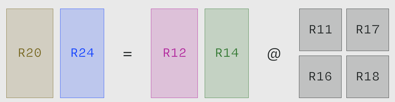
- Instructions 1 and 2 multiply the first eight columns of input
a(fromR12) by the first eight rows of inputb(fromR11andR17). The result is a 16 × 16 matrix stored inR20andR24. This is a kind of "outer product": a tall, skinny matrix times a short, wide one.RZis a special-purpose "register" holding the valueZero. - Instructions 3 and 4 compute the same kind of "outer product" for the second eight columns of
aand second eight rows ofb, accumulating onto the output of the first two to produce the finalc.
Put another way: for a block of eight rows and eight columns of B and an entire column of A, the Tensor Core performs many multiplications and additions concurrently within a single instruction. Each instruction handles all m rows of A for its block of B. Together, the instructions cover the full matrix multiplication.
To dig deeper, explore this compiler output on Godbolt. Note that this is far from a utilization-maximizing Tensor Core matrix multiplication. For that, see this worklog by Pranjal Shandkar.
Programming Tensor Cores in practice#
Hopper and Blackwell Tensor Cores can't be programmed for maximum performance in pure CUDA C++. They need PTX intrinsics for both computation and memory. The usual recommendation is to use existing kernels from libraries like cuBLAS (CUDA Basic Linear Algebra Subroutines), or higher-level kernel programming interfaces like CUTLASS (CUDA Templates for Linear Algebra Subroutines) in C++ or CuTe DSL in Python.
Hardware facts#
- Tensor Cores are much larger and less numerous than CUDA Cores. An H100 SXM5 has only four Tensor Cores per SM, one per Warp Scheduler, but hundreds of CUDA Cores.
- Tensor Cores are the primary producers and consumers of Tensor Memory.
- They were introduced in the V100 GPU, a major step in making NVIDIA GPUs suitable for large neural network workloads. See NVIDIA's V100 white paper.
- Their internals are unknown and likely differ between SM architectures. They are commonly assumed to be systolic arrays, like TPUs, but there is no consensus in the microbenchmarking literature.
Related#
- CUDA Core: the scalar counterpart
- Tensor Memory: dedicated storage for Tensor Core operands
- Warpgroup: the thread group used by newer Tensor Core instructions
- CUTLASS: the practical way to program Tensor Cores