L1 Data Cache
The private on-chip SRAM memory of each Streaming Multiprocessor, partitioned among its thread blocks and largely managed by the programmer.
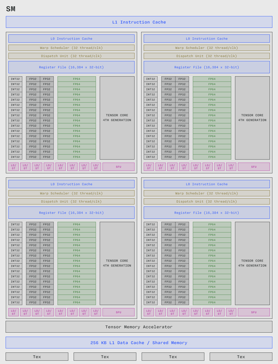
The L1 data cache is the private memory of a Streaming Multiprocessor (SM). Each SM partitions it among the groups of threads scheduled onto it.
Speed and implementation#
The L1 data cache sits next to the components that perform computation (e.g. the CUDA Cores) and is only about an order of magnitude slower than them.
It is built from SRAM, the same basic semiconductor cell used in CPU caches and registers and in the memory subsystem of Groq LPUs. The SM's Load/Store Units access it.
Programmer-managed#
Key idea CPUs have an L1 cache too, but it is fully hardware-managed. On GPUs, the L1 cache is mostly programmer-managed, even in high-level languages like CUDA C.
Capacity on H100#
| Capacity | |
|---|---|
| Per SM | 256 KiB (2,097,152 bits) |
| Across 132 SMs (H100 SXM 5) | 33 MiB (242,221,056 bits) |
Related#
- Shared Memory: the programming-model view of this cache
- Register File: the faster memory one level closer to the cores
- GPU RAM: the large, slow memory at the other end
- Bank Conflict: a common performance pitfall when using it